Complete Eagle CAD PCB Design: Theory and Practical approach
Complete PCB Design Course for Freshers & Professionals.
Summary
- Reed Courses Certificate of Completion - Free
- Tutor is available to students
Add to basket or enquire
Overview
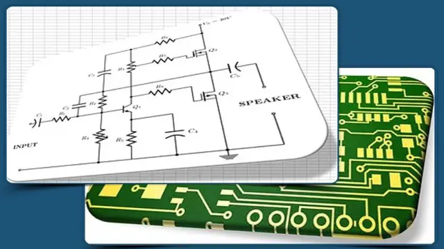
PCB Design and electronics circuit are basements for all type of electronics products. PCBs are derived from the analog and digital circuits which are prepared according to the application required. Printed circuit boards are the main pillars of the Electronics world. Every Electronics products has PCB inside it, from consumer gadgets like computers, smart phones and gaming consoles to industry and even high-tech products.
The key points are...
- You will learn Basic Electronics Theory, Circuit Design and Analysis, Basics of Printed Circuit Board, Electronic Components and Instruments. Study notes given.
- You will work on Printed Circuit Board Layout Design such as Schematic creation, Library Creation: Electronic Symbol and Package (Footprint Creation) Designing.
- Switching schematic to Board Design (Netlist Creation), Thorough knowledge on Constraint Management Settings, Board Shape Creation (DXF import included) & DRC.
- Work on Single sided Board Design, Double sided Board Design, Via creation and application. Routing on Top and Bottom Layer includes enough practice modules.
- Plan Creation of Power and Ground. Also Split Plan Creation. Design Rule Checking and DRC updates. Work on Artwork. Setting up all required film layer setups.
- Gerber Generation and Gerber analysis and improvements. PCB Manufacturing overview.
Certificates
Reed Courses Certificate of Completion
Digital certificate - Included
Will be downloadable when all lectures have been completed.
Curriculum
Course media


Description
PCB Design and electronics circuit are basements for all type of electronics products. PCBs are derived from the analog and digital circuits which are prepared according to the application required. Printed circuit boards are the main pillars of the Electronics world. Every Electronics products has PCB inside it, from consumer gadgets like computers, smart phones and gaming consoles to industry and even high-tech products.
Skills you gain after the course completion:
Basic Electronics and Electronic components expertise.
Circuit Designing (Power management circuit designing)
Circuit Simulation for best understanding of the subject.
Tools/Software Expertise.
Basic design module practice.
Advanced design module practice.
Library Module:
o Symbol and Footprint design for all types of packages.
High speed placements & routing techniques.
Design for Manufacturing, Testing and Fabrication expertise.
Gerber generation and editing.
Benefits of choosing PCB Design Course:
Strong hold in basic electronics.
Circuit Design capability.
Circuit analysis & ERC.
Components knowledge.
Power Supply designing.
Power Integrity Analysis.
Multiple PCB-CAD tool expertise.
Expert in library creation.
Multi-layer PCB designing.
Gerber creation & editing.
Who is this course for?
This course is for...
- Diploma in Electronics and Communication, Diploma in Electronics and Electrical and Diploma in Electrical.
- Bachelor of Engineering in Electronics and Communication, Bachelor of Engineering in Electrical and Electronics.
- BSc in Electronics, MSc in Electronics, MS in Electronics and Post graduate in Electronics and communication.
- Hardware designers, PCB manufacturer, Electronic Components engineer, PCB design and developers.
- Circuit designers, Embedded engineers and Beginners interested in development of PCB
Requirements
Prerequisites for taking your course are...
- Basic Electronics knowledge, BSc(Electronics), Diploma (Electronics or Electrical), BE (Electronics or Electrical), Master degree in Electronics and Electrical
- If you are working in PCB Manufacturing and Assembly unit, PCB Design course will be an added skillset to your career profile.
- If you own PCB printing, assembly and component soldering unit, you can learn PCB Design and can extend your business unit towards service sector.
- If you have passion on Electronics subject, you can enroll this course and convert your passion into career.
Career path
PCB designers can work in various industries, including electronics, communication and manufacturing. A PCB designer is a technical professional who uses computer software programs to design the layout for circuit boards. Landing a job as a PCB designer can be both worthwhile and rewarding. PCB designers can make up to $100,000 per year, and the career field is expected to grow 2% by 2028.
Questions and answers
Currently there are no Q&As for this course. Be the first to ask a question.
Reviews
Currently there are no reviews for this course. Be the first to leave a review.
Provider
I hold degrees in Electronics and Communication Engineering. I am an Electronics and Communication Engineer that specializes in circuit design, hardware design, PCB layout design and PCB Manufacturing. I have written many blogs and articles on the aforementioned subjects and taught Electronics Engineering courses at Swarna Institute of Technology (recognized by Micro Small and Medium Enterprise (MSME), Government of India) as well as online for many years.
I also train on many professional skills like Microsoft office (Microsoft Word, Microsoft presentation and Microsoft Excel etc.), Fusion 360 (3D design and Development), Website Design and Development, Digital Marketing and 2D and 3D Animation. I am currently working as 'Training Head' at Swarna Institute of Technology, Bangalore, Karnataka, India.
Add to basket or enquire
Legal information
This course is advertised on Reed.co.uk by the Course Provider, whose terms and conditions apply. Purchases are made directly from the Course Provider, and as such, content and materials are supplied by the Course Provider directly. Reed is acting as agent and not reseller in relation to this course. Reed's only responsibility is to facilitate your payment for the course. It is your responsibility to review and agree to the Course Provider's terms and conditions and satisfy yourself as to the suitability of the course you intend to purchase. Reed will not have any responsibility for the content of the course and/or associated materials.
